EV Chargers - 2W & 3W
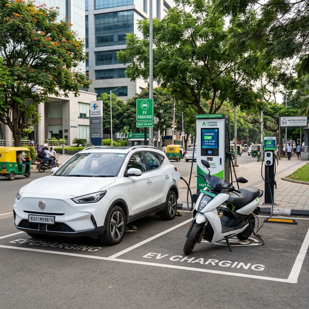
India's highest-volume electric mobility segment. OEMs in active redesign cycles for high power density onboard chargers.

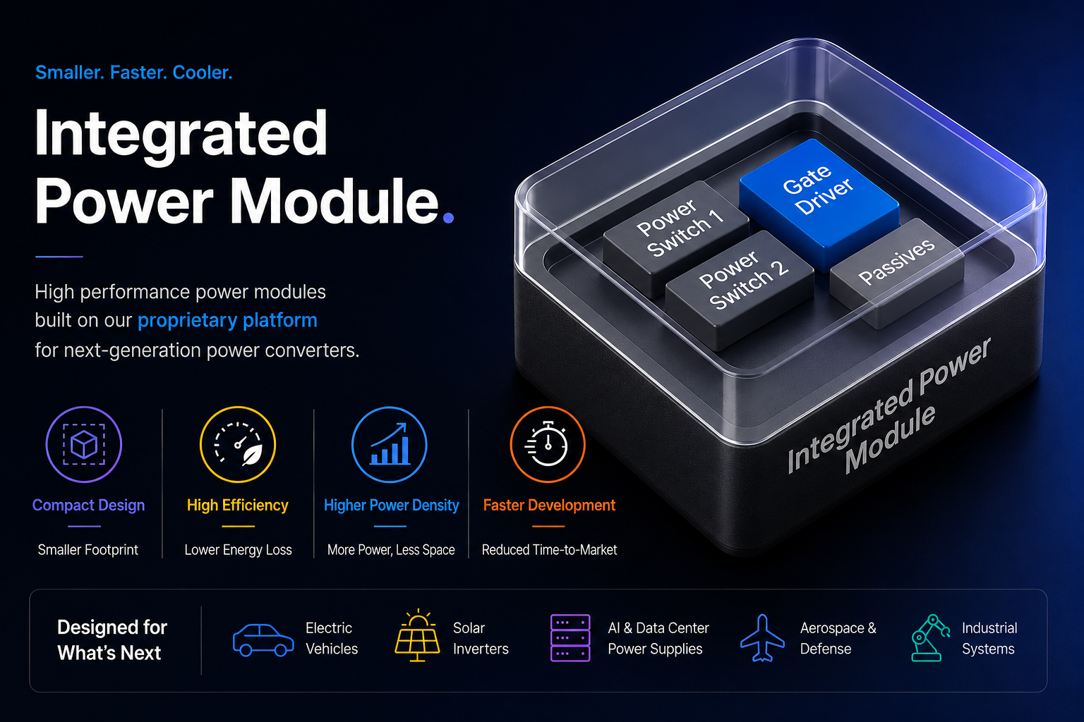
At Ganesis Semiconductors, we develop High Power Silicon Interposer (Si-IP) that integrates power switches (GaN, SiC or Si) and gate drivers directly on a silicon substrate - eliminating the parasitic inductance and thermal bottlenecks that prevent wide-bandgap semiconductor devices from reaching their potential.
 Smaller Footprint
 Lower Energy Loss
 More Power, Less Space
 Reduced Time-to-Market
 Electric Vehicles
 Solar Inverters
 AI & Data Center Power Supplies
 Aerospace & Defense
 Industrial Systems



Wide-bandgap power devices switch up to ten times faster than silicon at equivalent voltages, enabling smaller passive components, higher power density, and lower switching losses. Yet in practice, power converters built with these devices remain bulky and require active cooling. The reason is not the semiconductor. It is the circuit board connecting it.
For a 100V rated device switching 90A at 30 A/ns: 3 nH generates a 90V spike, pushing the device to its limit. At 5 nH the spike exceeds the blocking voltage. To survive, switching speed must be reduced. The advantage that justified the device choice is lost.
In a conventional discrete PCB layout, the power switch and gate driver IC are physically separated by millimetres of copper trace. That separation carries unintended inductance, and inductance fights rapid current change. The faster the device switches, the larger the voltage spike the board generates in response.
PCB traces connecting the switch and driver are not ideal conductors. They carry unintended inductance proportional to the area of the current loop. At 5-10 nH, typical for discrete layouts, the board generates voltage spikes large enough to destroy the device or force engineers to slow switching speed, surrendering every wide-bandgap advantage.
Standard PCB substrates conduct heat 500 times worse than silicon. The faster the device switches, the more heat it generates, and FR4 cannot remove it fast enough. External cooling is added, eliminating every size and weight advantage the semiconductor offered.
Power switch pair, gate driver IC, bootstrap capacitors, gate resistors, thermal interface, each separately sourced, placed, and qualified. The longer the loop connecting them, the worse the inductance.
Even the best optimised discrete PCB layout cannot eliminate the physical separation between the switch and driver. As long as components are placed as individual parts on a board, the current loop carries inductance. The solution is co-packaging them on a single substrate, where the loop length is measured in micrometres, not millimetres.
Two high-current power terminals and a logic-level PWM input. Identical interface to a conventional discrete half-bridge. The difference is everything inside the package: no external parasitic management, no external thermal design, no multi-supplier qualification.
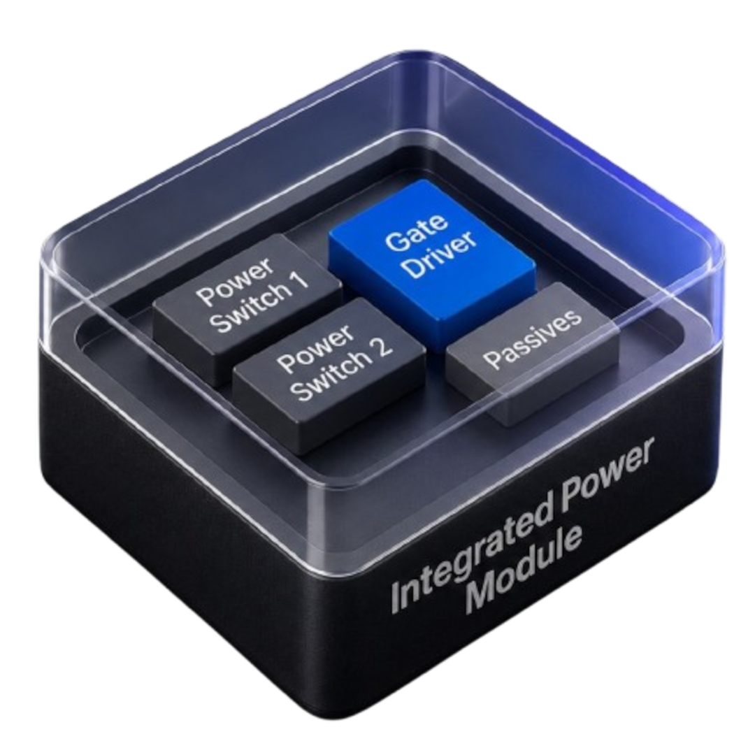
The GaNeSis Power Block co-packages the power switch, gate driver IC, and passive components directly on a silicon substrate, the High Power Silicon Interposer (Si-IP). By placing every component on the same substrate, the current loop shrinks from millimetres of PCB trace to micrometres of copper conductor. The inductance drops from 5-10 nH to below 1 nH. The PCB is no longer in the loop.
The Si-IP platform is designed from the ground up to support the full wide-bandgap roadmap as device technologies evolve.
Sub-1 nH power loop inductance, achieved by placing switch and driver on the same substrate, means the board no longer fights back. Power devices operate at their rated switching speed with no destructive voltage transients (engineering target).
Silicon conducts heat at 150 W/m-K, which is 500 times better than FR4's 0.3 W/m-K. Heat is extracted directly from the device junction through the substrate, significantly reducing the size of external cooling required compared to a discrete PCB layout.
One Power Block replaces the switch pair, gate driver IC, bootstrap capacitors, gate resistors, and thermal interface. That is 7 or more discrete components from multiple suppliers. One module. One datasheet. One qualification. One procurement line item.
The Si-IP substrate architecture is shared across GaN, SiC, and silicon integration. The layout is adapted for each device, but the platform, the thermal design, and the OEM interface remain consistent. Designs built on the Si-IP platform are not locked to a single semiconductor generation.
First-generation Power Block modules built on the Si-IP platform. Initial variants integrate GaN for EV and solar applications. The same platform architecture scales to SiC for higher-voltage traction and industrial applications.
Targeting EV onboard chargers and solar inverters. In active design-lock and fabrication stage at IISc Bengaluru.
Same Si-IP platform architecture. Higher-voltage traction and industrial applications. On the product roadmap.
GaN, SiC, and Si integration on the same substrate architecture. One platform. Every device generation.
The platform is in active design-lock and fabrication stage at IISc Bengaluru. Datasheets and evaluation kits will be available following prototype validation.
B2B component supply to OEMs across four high-growth power electronics verticals. First-generation modules use GaN. The Si-IP platform extends to SiC and Si variants as OEM requirements dictate. The customer is an engineer or procurement lead, not an end consumer.
View Full Datasheets arrow_forward
India's highest-volume electric mobility segment. OEMs in active redesign cycles for high power density onboard chargers.

GPUs demand over 800A per rack. Next-gen 48V point-of-load converter designs require ultra-low inductance modules. Si-IP platform is a direct fit for vertical power delivery architectures.
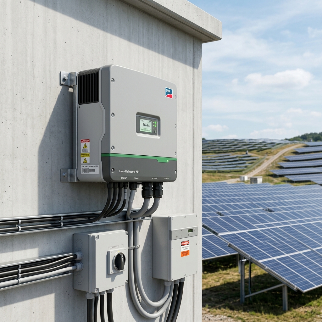
National Solar Mission and PM Suryodaya Yojana driving rapid expansion. Wide-bandgap inverters command an efficiency premium: every 1% improvement reduces cost per watt.
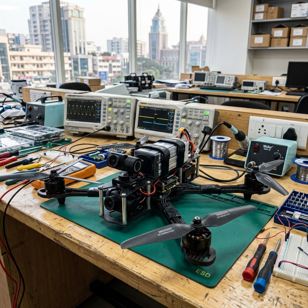
UAV and drone system manufacturers where size, weight, and power efficiency are primary design constraints. Motor drives and servo systems transitioning from silicon IGBTs to wide-bandgap devices.
Initial prototype validation of the platform.
First fully functional integrated module.
OEM ready prototypes
GaNeSis Semiconductors is a deep-tech startup building a semiconductor-agnostic advanced packaging platform for high-performance power electronics. Based at IISc Bengaluru, the company develops the High Power Silicon Interposer (Si-IP), co-packaging power switches and gate drivers into a single system-ready module.
The Si-IP addresses the packaging barrier that prevents GaN, SiC, and silicon devices from reaching their theoretical potential, targeting OEMs in EV power systems, solar inverters, AI data centres, and industrial power electronics.
To become the foundational semiconductor integration platform for high-performance power electronics, enabling wide-bandgap devices to reach their theoretical potential across EV, AI infrastructure, renewable energy, and industrial applications at global scale.
To eliminate the packaging barrier that prevents wide-bandgap semiconductors from replacing silicon in high-performance power conversion. GaNeSis builds the integration layer that sits above the chip and below the system, making the next generation of power electronics smaller, more efficient, and thermally superior.
India's premier institute for research and advanced education in science and engineering. GaNeSis is incubated at CeNSE, IISc's Centre for Nano Science and Engineering.
Gallium Nitride Ecosystem Enabling Centre and Incubator at IISc. India's dedicated wide-bandgap technology incubator providing fabrication access and deep-tech mentorship.
Foundation for Science Innovation and Development. IISc's technology incubation and IP commercialisation arm supporting deep-tech ventures from research to market.
Together, this ecosystem provides GaNeSis with world-class wide-bandgap fabrication infrastructure, academic expertise across semiconductor physics and power electronics, and a proven pathway from research to commercial product.
In-depth technical resources for evaluation and integration.
Comprehensive technical overview of the Ganesis Si-IP architecture, thermal simulation data, and electrical performance benchmarks.
Application-specific integration guide for EV, solar, data center, and industrial power conversion systems.

Founder & Chief Executive Officer
PhD candidate developing GaN power devices and advanced power module architectures at CeNSE, IISc.

Technical Advisor
Professor at CeNSE, IISc. Expert in 3D heterogeneous integration and advanced semiconductor packaging technologies.

Technical Advisor
Professor at IISc. Specialist in high-frequency power converter topologies, modulation, and closed-loop control.
Whether you are an OEM evaluating integration, an investor exploring the platform, or a researcher interested in collaboration — we are ready to talk.
Thank you. Our team will contact you shortly.